
 Sign in
SWAP provides images of the solar corona at about 17.4 nm, a bandpass that corresponds to a temperature of roughly 1 million degrees, with a cadence of 1 image per 1-2 minutes, and field of view (FOV) of 54 arcmin.
Several major innovations have been introduced in the design of the instrument in order to be compliant with the requirements of the PROBA2 micro-satellite: compactness, with a new off-axis optical design, radiation resistance with a new CMOS-APS detector, a very low power electronics, an athermal opto-mechanical system, optimized onboard compression schemes combined with prioritization of collected data, autonomy with automatic triggering of observation and off-pointing procedures in case of solar event occurrence.
All these new features result from the low resource requirements (power, mass, telemetry) of the mini-satellite, but also take advantage of the specificities of a modern technological platform, such as quick pointing agility, new powerful on-board processor, Packetwire interface, and autonomous operations.
Detector and Focal Plane Assembly
The detector is a technologically advanced CMOS (Complementary Metal Oxide Semiconductor) device coated with a scintillator layer to improve sensitivity in the EUV range. It has 1024 by 1024 pixels, each pixel having a 18 µm x 18 µm size.
This particular type of detector, called "High Accuracy Startracker" (HAS), is a radiation hardened, active pixel sensor (APS) detector.
The detector will be passively cooled with an external radiator viewing cold space to reduce thermal noise. This type of detector offers great advantages for space-based solar EUV imaging: radiation resistance, improved noise reduction, shutterless operation, and non destructive readout.
The focal plane assembly will also include the proximity electronics required to readout the sensor, a set of calibration lamps and a radiator viewing cold space to cool the detector through a cold finger. An additional feature is the decontamination heater, which will be used periodically to out-gas the condensed layer that builds up on the cold sensor (= bake-out process). Such deposits can absorb EUV radiation and dramatically decrease photon throughput.
The optical and focal plane assemblies will be mounted on an optical bench designed to provide mechanical stability and insensitivity to thermal variations. A lightweight invarstructure will provide a degree of stability better than 50 µm between SWAP's two mirrors.
Properties of the CMOS APS Detector
The CMOS ‘active pixel sensor' (APS) detector has been developed as an alternative for CCD detectors in high-resolution, efficient digital X-ray and EUV imaging. In general, the use of CMOS technology offers several advantages over CCD technology:
- Every pixel can be read out separately so no shutter is needed.
- The power supply needed for a CMOS detector is negligible. This is important for SWAP since there are only 5 Watts available for the whole instrument.
- Camera-on-chip integration (camera control and interface logic is integrated on the chip)
The use of ‘active pixels' largely optimizes the image quality which was - in the past - much lower in CMOS detectors than for CCD cameras. The integration of the amplifier inside the pixel results in low noise and a high light-to-voltage conversion gain. The usual drawbacks of this approach, a low photon-charge conversion and pixel non-uniformities or fixed pattern noise, are eliminated in the SWAP detector by using a pixel structure with a high fill factor and a compensation circuit for fixed pattern noise.
How Do SWAP's Active Pixels Work?
Making a direct digital image involves converting the EUV radiation into a digital signal, which is a multi-step process:
- A conversion screen - the scintillator coating - is exposed to radiation and converts the EUV radiation into visible light.
- The pixel, in direct contact with the screen, converts the light into electrons that are then stored in a capacitor (voltages go down).
- When the capacitor discharges, the current is sent to an amplifier. Each CMOS pixel is configured with its own amplifier, a significant improvement over CCD detectors in which only one amplifier is available for each row of pixels in the array.
- The amplifiers are switched on and off by timing and control circuitry right on the chip, making additional circuitry adjacent to the panel unnecessary.
- The last step of the process is to perform analog-to-digital conversion of the signal that is done right at the sensor. In this process, the analog signal is converted into 12-bit binary code.
Scintillator coating
The scintillator layer on top of the CMOS detector consists of the phosphorus called "P43" which converts EUV radiation to visible light by the process of scintillation. The incoming radiation is absorbed (in this case EUV radiation at 17.5 nm) and light of a longer wavelength (visible light at 545 nm) is re-emitted, releasing the previously absorbed energy. The re-emitted visible radiation can then be detected by the active pixels of the CMOS detector. P43, the specific scintillator coating used in the SWAP detector, is a phosphorus made of the host material Gd2O2S which gets activated by Td.
Detector efficiency
The image is built assigning to each pixel a discrete value called DN (Digital Number) made by converting the analog signal to digital values. The DN/photon relation is:
DN = NUVphotons.QEP43.QECMOS.Gampli.GADC
where:
NUVphotons = number of UV photons reaching the coating surface [phUV]
QEP43 = scintillator efficiency [phVIS/phUV]
QECMOS = detector efficiency [e-/phVIS]
QE = QEP43.QECMOS = overall quantum efficiency of the coated detector [e-/phUV]
Gampli = gain of the programmable amplifier [V/e-]
GADC = gain of the analog-to-digital converter [DN/V]
OG = Gampli.GADC = overall gain of the detector [DN/e-]
The overall efficiency of the HAS APS is:
0.0186 DN/photon +/- 10% at 633 nm.
The quantum efficiency of the CMOS detector and the P43 coating separately are:
QECMOS = 0.45 e-/ph +/- 10%
QEP43 = 2.1 phVIS/phUV
so that the overall quantum efficiency of the coated detector at 17.5 nm is: QE = 0.945.
The largest signal that the sensor can capture is equal to 2493 DN.
SWAP will image a square field of view of 54 arcmin on 1024x1024 pixels, using an off-axis telescope derived from a Ritchey-Chretien system. An elliptical primary mirror combined with a spherical secondary mirror used in quasi-normal incidence will focus the solar light on a technologically advanced CMOS detector, implemented in a focal plane assembly. A set of optical planar baffles will avoid unwanted stray light onto the detector.
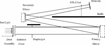
- General overview of the SWAP optical path

The overall optical elements are mounted on an optical bench to provide the necessary stability. The spectral selection is achieved with a set of aluminum foil filters, together with EUV reflective multilayer coatings deposited on the mirrors. The two aluminum filters are both supported, the front filter by a polyimide membrane and the rear filter by a nickel grid. The grid will cause an artificial pattern on the detector but since it is only present in the rear filter (which is the closest to the focus) no diffraction patterns will be visible.
The instrument is encased in a light weight housing equipped with an aperture mechanism to preserve the optical cavity from external contamination during on-ground activities and the launch phase. SWAP is mounted on the spacecraft platform with a set of isostatic flexible mounts.
The optics are manufactured and polished to a microroughness below 0.5 nm, then glued into dedicated mounts and coated. The optical coating is a multilayer composed by about 30 alternating layers of two different materials (Mo and Si). The overall stack is specifically designed to provide reflectivity in the extreme ultraviolet range, and to achieve the spectral selection in a narrow band pass (1.5 nm) centered on 17.5 nm. The accuracy on central wavelength adjustment is within +/- 0.2 nm.
SWAP On-board Operations
SWAP data will benefit from series of innovations that have been implemented during the development of the instrument and platform flight software. Most of them can be considered as demonstrators for future space missions.
PROBA2 will fly with the new 100 MHz AT697 LEON II microprocessor. It will be the first satellite mission to fly ESA's new high performance, radiation hardened processor which is expected to be used for many other ESA missions such as Solar Orbiter. The extra computing power delivered by the new microprocessor will make possible to implement some basic on-board image processing capabilities dedicated to SWAP data, and benefit from some automatic processing and autonomous operations.
The SWAP images are stored in the MCPM. Before being compressed, discontinuities (cosmic rays) are removed and weak pixels are compensated by on-board routines based on flat field information. These operations will avoid JPEG compression artefacts. When JPEG algorithm is selected, the 12-bit pixel values are re-coded to 8-bit before compression. A sophisticated re-coding12 algorithm is used to minimize the data alteration.
When default imaging mode is used with full images at 1-minute cadence, SWAP will produce more data than what can be sent to the ground stations. An automatic data prioritization process has been defined in order to make the best use of the limited telemetry bandwidth. This algorithm aims to identify potentially interesting solar events and transfer the associated data to the ground in higher priority.
An interesting feature of PROBA2 has been diverted to improve the coronal mass ejection (CME) observation program. PROBA2 is a 3-axis stabilized platform with agile capabilities. This means that PROBA2 can quickly change the pointing of SWAP in any direction. The nearly real time on-board processing of the SWAP images will allow detecting eruptions of material from the Sun's surface in a set of predefined sectors. When any of such event is detected, SWAP MCPM triggers an off-pointing procedure, in order to follow the CME in a given direction. This exploratory mode will enlarge the field of view of SWAP by a factor 3, although the instrument has straylight limitations as well as relatively limited throughput for faint EUV emissions observed from CMEs. Such event detection can also trigger an increase in temporal cadence and a specific windowing mode that will give access to scientific analysis of the first stage of CME accelerations.